-
Breakthrough Digital Lithography Technology From Applied Materials and Ushio to Enable More Powerful Computing Systems for the AI Era
Источник: Nasdaq GlobeNewswire / 12 дек 2023 15:05:22 America/Chicago
- Strategic partnership to accelerate industry’s transition to heterogeneous chiplet integration on glass and other large substrates
- Partnership combines Applied’s leadership in large panel processing with Ushio’s leadership in lithography for packaging
- New digital lithography technology to enable world’s leading chipmakers to combine chips with sub-micron wiring
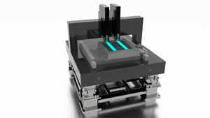
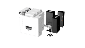
SANTA CLARA, Calif. and TOKYO, Dec. 12, 2023 (GLOBE NEWSWIRE) -- Applied Materials, Inc. and Ushio, Inc. today announced a strategic partnership to accelerate the industry’s roadmap for heterogeneous integration (HI) of chiplets into 3D packages. The companies are jointly bringing to market the first digital lithography system specifically designed for patterning the advanced substrates needed in the Artificial Intelligence (AI) era of computing.
Rapidly growing AI workloads are driving the need for larger chips with greater functionality. As the performance requirements of AI outpaces traditional Moore’s Law scaling, chipmakers are increasingly adopting HI techniques that combine multiple chiplets in an advanced package to deliver similar or higher performance and bandwidth as a monolithic chip. The industry needs larger package substrates based on new materials such as glass that enable extremely fine-pitch interconnects and superior electrical and mechanical properties. The strategic partnership between Applied and Ushio brings together two industry leaders to accelerate this transition.
“Applied’s new Digital Lithography Technology (DLT) is the first patterning system that directly addresses the needs of our customers’ advanced substrate roadmaps,” said Dr. Sundar Ramamurthy, Group Vice President and General Manager of HI, ICAPS and Epitaxy, Semiconductor Products Group at Applied Materials. “We are leveraging our unmatched expertise in large substrate processing, the industry’s broadest portfolio of HI technologies, and deep R&D resources to enable a new generation of innovation in high-performance computing.”
“Ushio brings over 20 years of experience building lithography systems for packaging applications, with more than four thousand tools delivered worldwide,” said William F. Mackenzie, Group Executive Officer and General Manager, Photonics Solutions Global Business Unit at Ushio. “With this new partnership, we can accelerate adoption of DLT through our scalable manufacturing ecosystem and robust field-service infrastructure, and broaden our portfolio to provide more solutions to the rapidly evolving challenges in packaging technology.”
The new DLT system is the only lithography technology that can achieve the resolution necessary for advanced substrate applications while delivering throughput levels required for high-volume production. With the ability to pattern less than 2-micron line widths, the system enables the highest area density for chiplet architectures on any substrate, including wafers or large panels made of glass or organic materials. The DLT system is uniquely designed to solve unpredictable substrate warpage issues and achieve overlay accuracy. Production systems have already been shipped to multiple customers, and 2-micron patterning has been demonstrated on glass and other advanced package substrates.
Applied pioneered the technology behind the DLT system and will be responsible for R&D and definition of a scalable roadmap together with Ushio to enable continued innovation in advanced packaging to 1-micron line widths and beyond. Ushio will leverage its mature manufacturing and customer-facing infrastructure to accelerate adoption of DLT. Together, the partnership offers customers the broadest portfolio of lithography solutions for advanced packaging applications.
Forward-Looking Statements
This press release contains forward-looking statements, including those regarding anticipated growth and trends in our businesses and markets, industry outlooks and demand drivers, the benefits of the Digital Lithography Technology (DLT) and the partnership between Applied and Ushio, our market opportunities for advanced packaging lithography and other technologies, and other statements that are not historical facts. These statements and their underlying assumptions are subject to risks and uncertainties and are not guarantees of future performance.Factors that could cause actual results to differ materially from those expressed or implied by such statements include, without limitation: the level of demand for the DLT; failure to realize the anticipated benefits of the partnership between Applied and Ushio; global economic, political and industry conditions; the introduction of new and innovative technologies, and the timing of technology transitions; our ability to develop, deliver and support new products and technologies; market acceptance of existing and newly developed products; our ability to obtain and protect intellectual property rights in key technologies; our ability to accurately forecast future results, market conditions, customer requirements and business needs; and other risks and uncertainties described in our SEC filings, including our recent Forms 10-K, 10-Q and 8-K filed with the U.S. Securities and Exchange Commission. All forward-looking statements are based on Applied and Ushio management’s current estimates, projections and assumptions, and neither company assumes any obligation to update them.
About Applied Materials
Applied Materials, Inc. (Nasdaq: AMAT) is the leader in materials engineering solutions used to produce virtually every new chip and advanced display in the world. Our expertise in modifying materials at atomic levels and on an industrial scale enables customers to transform possibilities into reality. At Applied Materials, our innovations make possible a better future. Learn more at www.appliedmaterials.com.About Ushio
Ushio Inc. (Head office: Tokyo, TSE: 6925) Established in 1964. The company manufactures and sells lamps, lasers, light emitting diodes, and other light sources in the ultraviolet, visible, and infrared bands of the spectrum along with optical and imaging equipment incorporating these devices. Numerous Ushio products in the industrial processes field, which encompasses the manufacturing of semiconductors, flat panel displays, electronic components and other products, and in the visual imaging field, characterized by digital projectors, illumination, and other products, have large market shares. In recent years, Ushio’s operations have expanded to the life sciences field, most notably medical applications and the environment. https://www.ushio.co.jp/en/Applied Materials Contacts:
Ricky Gradwohl (U.S. editorial/media) 408.235.4676
Yuji Hotta (Japan editorial/media) +81-3-6812-6820
Michael Sullivan (financial community) 408.986.7977Ushio Contacts:
Corporate Communication Department (Japan editorial/media) +81-3-5657-1017
Shintaro Yabu (U.S. editorial/media) 714.229.3189Photos accompanying this announcement are available at:
https://www.globenewswire.com/NewsRoom/AttachmentNg/815b368c-75a3-4ab1-8a14-76971688ca86
https://www.globenewswire.com/NewsRoom/AttachmentNg/7f5c3a22-41e5-4b3b-8842-7923cb4de0a2

Digital Lithography Technology (DLT)
New digital lithography technology from Applied Materials and Ushio to accelerate the computer industry’s transition to heterogeneous chiplet integration on glass and other large package substrates.
Digital Lithography Technology (DLT)
Applied Materials and Ushio are introducing a breakthrough digital lithography system for glass and other large package substrates that enables high-performance heterogeneous chip designs for the AI era of computing.


